How Electronic Tattoos are made via nanotechnology

Electronic tattoos are a new and advanced approach to nanotechnology. They are an invention of the biomedical field. For this purpose, printed electronics are used which have suitable properties that fit the demands of electronic tattoos. The less damaging agents are used as an alternative to reduce the harms that a tattoo can cause.
Nanotechnology is a process and field in which nanoparticles are involved. They are highly efficient and have very effective properties that make them highly usable in all the different fields of life. Researchers also believe that nanotechnology is going to be proved very effective for the economy in all aspects.
Introduction
The innovation and research field which is concerned with the formation of things, like devices and materials, on a molecular and atomic scale is known as Nanotechnology. The 1 billionth of a meter is a nanometre and its diameter is 10 times more than a hydrogen atom. On average, the human hair’s diameter is 80,000 nanometres. The normal rules of chemistry and physics don't apply on such scales. For example, the properties of materials, for instance, their strength, reactivity, conductivity, and color are considerably different between the macro and the nanoscale. As compared to steel, carbon nanotubes are 6 times lighter but still 100 times stronger.
The consumption of energy can be increased by nanotechnology, it can also aid in environmental clean-up and in solving significant health problems. It is said that at very fewer costs, it can highly increase manufacturing production. Despite being more functional, nanotechnology products are lighter, cheaper, and smaller. According to the advocates of nanotech, they need less raw materials or energy for the manufacturing process.
It is hoped by many governments that a new era of wealth and productivity will begin with nanotechnology. The public also supports this vision as it is assured by the fact that in the past decade, the public investment in the development and research of nanotechnology has risen.

Properties
Nanoparticles have principal parameters which are their size, shape (containing aspect ratios), and the substance’s morphological sub-structure. The nanoparticles are displayed as an emulsion (two liquid phases), as a suspension (mostly solid in liquids), or an aerosol (mostly liquid or solid phase in the air).
The interfacial and surface characteristics may modify in the chemical agent's presence (surfactants). Such agents can indirectly stabilize against aggregation or coagulation by preserving the charge of the particle and by the modification of the particle's outermost layer. The nanoparticle’s lifetime and growth history determine the complex compositions and absorbates complex mixtures. Various agents are disposed to condensation on the particle while it is cooled down and then opened to various ambient atmospheres.
Only a small amount of particulate model systems have complex surface chemical processes. Between the micrometer scale and the Angstrom level, at some point the nanoparticle’s simple picture as a droplet or ball changes. In a complex method, both chemical and physical characteristics are derived from the molecular and atomic origins.
For instance, as compared to the components at extended surfaces or in the bulk, the chemical reactivity, optical, and electronic characteristics of small clusters are totally different. For predicting the evolution of such features, there is a requirement for complex quantum mechanical models with the size of the particle, and typically very well-defined conditions are required for comparing theoretical and experimental predictions.
How Electronic Tattoos work with nanotechnology
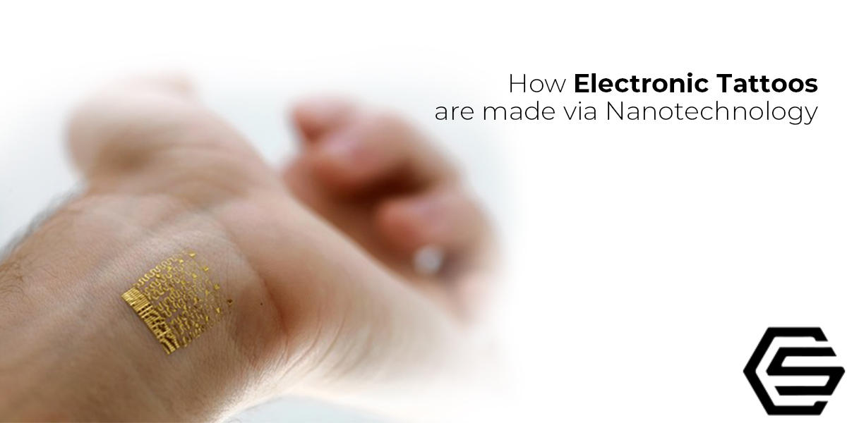
To create bio-interfacing electronics, the low-cost and flexible approach is the electronic tattoo as they gained a lot of attention recently in the field of bio-medicine. There are various publications on this topic, having their main focus on the sensors to light-emitting diodes, the transistors. The skin conforming electronic devices which are the fabrication of electronic tattoos (epidermal electronics) are in the description of many reports. For the purpose of the production of electronic tattoos, printed electronics are preferably suitable because of their compatibility with low-cost fabrication, customizability, and flexible substrates. Intricate electronics can be created by electrically conductive inks even though the materials and structures may vary between devices, the common feature remains the electrically conductive inks. Although to obtain low resistivity films, there is a standard requirement with printable conductive inks is one of the forms of relatively harsh post-processing.
There are different techniques in the printing conductive ink’s post-processing. The techniques include soaking or rinsing in dangerous chemicals, annealing/sintering at increased temperatures (>70 °C), exposure to laser sintering, or UV radiation. Direct printing on the epidermis is prevented by these tough conditions, opening the path for huge developments and changes in the treatment with electronics or patient-specific monitoring areas. Therefore, almost all the bio-interfacing electronics are totally made-up of substrates that are disposable and are transferred subsequently to a biological surface. Because of probable inconsistencies and problems in transferring, this transfer method is less than ideal, as it could alter the performance of the device, its lifetime, and its particular location for the most desired/sensitive operation.
To enable the biomedical devices of next-generation electronic tattoos form, the key is the development of conductive printable inks that at low temperatures are curable. Despite the direct-write printing onto sensitive biological surfaces, electronic tattoos' seamless incorporation also requires flexibility of high level and the capability of withstanding the bending strain that’s repetitive and is caused by the movement of everyday life.
Inspirable performance of bending was demonstrated in the past reports on low-temperature printed conductive traces. An important development is seen towards a seamless bio-interface with electronics. Russo et al. made an ink having a bending performance that’s superior to others but at room temperature, it needed an extended time to dry in addition to using cytotoxic nanoparticles whereas an ink having a rapid dry time was demonstrated by Zhu et al. but its bending performance was poor. A robust printed electronic tattoo can only be created when such a printing approach and ink are developed which have both optimal bending performance and rapid curing time, as only such properties have the potential of such creation with an extended lifetime.
The creation of this enhanced hybrid is possible through one method which is using the high aspect ratio electronic materials as the ink’s functional component. In comparison with AgNPs of similar diameter, silver nanowires (AgNW) have less cytotoxicity and are a high aspect ratio nanomaterial. The cytotoxicity of AgNW lessened even more when interacting as a thin film with cells.
Therefore, as a less damaging AgNP alternative, AgNW inks can be used. A promise is made by them to achieve high conductivity printed traces and it's being seen that their conductivity is maintained even when there is a bent underlying substrate. Moreover, at comparatively hot temperatures like 70 C, the creation of conductive solver nanowire networks take place with minimal post-processing and with conductivities orders of magnitude higher than that of AgNP (silver nanoparticles. Although, at temperatures above 38-40 C, biological materials start degrading rapidly. At others' expense, one of these advantageous features (low bending performance and low printing temperature) are delivered with inks frequently. Therefore, when printed near or at room temperature, high conductivity is maintained by ink which is capable of a truly seamless interface with a biological substrate.
Silver Nanowire Printing
For printing all silver nanowire films and traces, a nozzle of 200 µm diameter was used and for such printing, the speed of the print was 1 mm s−1. Print to print, there was a variation in the exact printing parameters for ensuring consistency in performance. 40-50 SCCM was the flow rate of the atomizer, 340-350 mA was the ultrasonic inducer current, and 25 SCCM was the used sheath flow. A nozzle of 150-200 µm diameter was used for silver nanowire printing and 3mm s-1 was the print speed. At 60°C platen temperature, the silver nanoparticle ink was printed and annealed for one hour at 200 °C in an oven.
To get more information about Silver Nanowires,
you can read blog post.
Instrumentation and Characterization
At the Duke Pathology Lab, film heights were measured, and SEM images were taken through the usage of an optical profilometer (Zygo NewView 5000) at the facility of shared materials instrumentation. Through the usage of the Keithley 2400 source measure unit and a 4-point probe method, the deposited films sheet resistance was measured.
Bend tests
At 20 C, by the usage of a 10 mg ml-1 formulation, the silver nanowire networks were printed for a total of 3 print passes with no additional processing. At 60 C, silver nanoparticle inks were printed and at 200 C, silver nanoparticle inks were annealed with 1 printing pass for 1 hour. For testing the resistance in states of both unbent and bent across the device, an Agilent Technologies B1500A Semiconductor Device Analyzer connected to a Signatone H100 tabletop probe station was used. A Kapton substrate of 127 µm thickness was used to perform all tests. A dowel with a required radius was used by hand as a guide to performing all bending tests. Also by hand, the repetitive cycling tests were performed to measure the resistance of the sheet after the completion of a bending cycle. In quadruplicate, each test was performed. Through the formula, ε = D/2R, the bending strain was calculated. In the formula, R is the bending radius, D is the substrate’s thickness, and ε is the bending strain. Therefore, when the substrate is folded in half, 50% bending strain occurs.
Basically, on the biological substrates, direct-write printing of conductive traces was enabled at room temperature by the biocompatible ink that is based on the silver nanowire. A short drying period is possessed by this ink, facilitating usage within some minutes of the printing. Also, nanowires' low-temperature printing helps in having optimal bending performance. This nanowire ink offers enhanced bending performance, higher adhesion to the substrate, and low-temperature curing than traditional silver nanoparticle inks.
By directly printing conductive traces onto a leaf, a human finger, and an apple, compatibility with sensitive biological surfaces was shown; in all instances, even though the major bending tests, a robust film having stable conductivity was yielded by the ink. The wearable electronics industry can be expanded with the assistance of this ink through incorporation with biocompatible integrated circuits via electronic tattoos that are directly printed, empowering very complex and useful bio-related sensors, trackers, and diagnostics.