Applications of 2D Nanomaterials Beyond Graphene

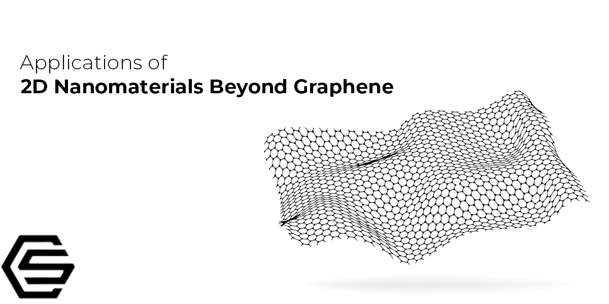
Graphene, a single layer of graphite, was the first 2D material that was discovered back in 2004. Graphene's success lead up to researchers to go beyond graphene.
Now, it has been made possible to create stable, single, and skinny layers of van der Waals materials. These advanced nanomaterials exhibit fascinating and technologically useful physical, chemical, and mechanical properties. 2D nanomaterials are generally ultra-thin materials and exhibit a high degree of anisotropy and chemical functionality. They are also highly diverse as far as their size, shape, biocompatibility, degradability, mechanical, chemical, and optical properties are concerned. Because of such distinct properties of the 2D nanomaterials, they are widely used in several applications such as drug delivery, imaging, tissue engineering, biosensors, and many other applications. Modern 2D nanomaterial nanotechnology is still in its infancy, but it is believed that it will revolutionize science, engineering, and technology in the coming years.
Introduction
Nanotechnology is the new face of the modern material sciences that is an engineering, technology, and science dealing with nanoparticles of extremely small size usually less than 100 nm. Nanotechnology involves the manipulation of individual atoms and molecules to achieve nanomaterials that exhibit phenomenal characteristics. Those characteristics of the achieved nanomaterials are significantly different from bulk materials. Nanotechnology has been a subject of extensive research in recent years because of its potential advantages in several other scientific fields such as material sciences, biology, chemistry, physics, and engineering.
Nanotechnology and nanomaterials are extremely useful and already have found use in a wide variety of potential applications in biomedical, biosciences, environmental protection, electronics, optics, etc. These materials have unique physical and chemical properties offering advantages on several fronts in the service of mankind. Nanotechnology completely changes the complexion of the bulk materials, making them more useful and highly advantageous than the bulk materials. That is the reason that nanotechnology is currently the focus of scientists. However, there is a lot to discover because "There is plenty of room at the bottom."
Two-dimensional nanotechnology materials are yet another miracle of modern nanotechnology. 2D materials are also known as single-layer materials. They consist of a single layer of atoms. These materials are extremely useful and have already found their uses in photovoltaics, semiconductors, electrodes, and water purification. 2D nanomaterials are materials with two dimensions outside the nanoscale. Such nanomaterials with thin layers and single-layer crystals have strong intralayer covalent bonding and weak interlayer van der Waals bonding that gives them superior electrical, optical, and mechanical properties.
2D materials have two categories, 2D allotropes of various elements and compounds. The -ene suffix is generally the part of the names of elemental 2D materials while 2D compounds carry -ane or -ide suffixes in their names. After discovering two-dimensional graphene, researchers embarked on a journey to seek other 2D materials such as metal carbides and nitrides. 2D silicon is one of the most interesting analogs to graphene. 2D boron is another material that can prove very handy in several applications. However, it is interesting to note that producing 2D materials beyond graphene is a very difficult and complicated process because other layered systems consist of two or more elements in contrast to graphene. Hence, there are certain challenges ahead that must be overcome to produce the desired 2D nanomaterials.
Is it possible to choose any material and thin it down to get a 2D material? Yes, it is possible, but many materials like diamonds have 3-dimensional chemical bonds that require cutting these bonds to get 2D structures. Such materials have high-density dangling bonds that are not chemically and energetically stable. That results in forcing materials to rearrange their structure to decrease their surface energy. Therefore, there are some special materials that can be used to get 2D materials of very high quality. There are two main methods to make 2D materials, top-down and bottom-up. The top-down approach involves starting with bulk materials and making them thinner. The bottom-up approach involves starting with the atomic ingredients and assembling them together to make 2D materials.
2D nanomaterials are generally ultra-thin materials and exhibit a high degree of anisotropy and chemical functionality. They are also highly diverse as far as their size, shape, biocompatibility, degradability, mechanical, chemical, and optical properties are concerned. Because of such diverse properties of the 2D nanomaterials, they are widely used in several applications such as drug delivery, imaging, tissue engineering, biosensors, and many other applications. In fact, 2D nanomaterials beyond graphene will be a gift of the 21st century to humankind.
History
Graphene, a single layer of graphite, was the first 2D material that was isolated back in 2004. That was a defining moment in the history of modern nanotechnology that opened the door for a new but unique field of 2D nanomaterials. In recent years, lots of research has been conducted to prepare 2D nanomaterials beyond graphene. MXene was the first 2D material beyond graphene that was discovered in 2011 at Drexel University. Silicene became the first post-graphene material to be discovered in 2012. Afterward, different 2D materials were discovered by researchers such as germanene, stanene, plumbene, etc.
What are 2D materials?
A total number of nanoscopic dimensions are used to classify nanomaterials.
Zero-dimensional or 0D have all three dimensions of nano size and are commonly known as nanoparticles.
One-dimensional or 1D has two dimensions of nano-size while the third dimension is much larger and is known as nanotubes or nanowires.
Two-dimensional or 2D have one zero-sized dimension and resemble a large thin sheet just like a piece of paper.
Finally, if a material doesn't have even a single zero-sized dimension, then that material cannot be branded as a nanomaterial and is considered bulk material.
Properties and Applications of Two-dimensional Nanotechnology Materials Beyond Graphene
2D nanotechnology materials exhibit phenomenal chemical, mechanical, and physical properties. They are ultrathin nanomaterial with an exceptional degree of anisotropy and chemical functionality. 2D materials are the thinnest materials and possess the highest surface area of all known materials making them highly suitable for all those applications that require high levels of surface interactions on a small scale.
Examples of 2D Materials Beyond Graphene
Graphene was the first 2D material isolated in 2004, and since then there have been many examples of 2D materials such as:
Hexagonal boron nitride is an isomorph of graphene, and it has a crystallographic appearance just like graphene. However, carbon atoms are replaced by nitrogen and boron in this unique 2D material.
Transition metal dichalcogenides is a 2D material that can adopt different crystal structures. The 2H-phase is the most common structure with trigonal symmetry that gives semiconductive characteristics. These are one of the most popular choices for 2D transistors.
Phosphorene is another example of 2D materials beyond graphene and is a direct bandgap semiconductor having a structure resembling a puckered honeycomb. The good charge mobility makes it highly useful for optoelectronic devices and transistors.
Xenes are monolayers of silicon, germanium, and tin with a hexagonal structure just like graphene. Although these 2D materials are still in their infancy, they are considered to have great potential for use in various applications.
Borocarbonitrides are 2D nanomaterials consisting of boron, nitrogen, and carbon atoms. These compounds have a high surface area and Stone-Wales defects in their structure. Both of these unique characteristics combine and allow a high absorption rate of CO2 and CH4, which makes borocarbonitrides highly useful for sequestering these gases.
Applications of 2D Nanomaterials Beyond Graphene
2D nanomaterials beyond graphene have also found their uses in various applications across several industries. The following is a list of some most promising applications of 2D nanomaterials other than graphene.
Transistors and sensors: Semiconducting 2D materials such as TMDCs and black phosphorus are used to fabricate field-effect transistors. Such 2D nanomaterials exhibit good charge mobility and moderate bandgap, making them exceptional candidates for this application.
Photodetectors: Having a bandgap in the optical or near-infrared region and good charge mobility properties of various TMDCs and black phosphorus are extremely useful for photodetectors.
Battery electrodes: Electrically conductive materials with a high surface area to volume ratio to store high densities of ions are phenomenal materials for electrodes used in ion batteries. Graphene is being used for this purpose. However, in recent years, 2D MoS2 has also gained significant attention in this regard. It is prepared in such a way that it develops a metallic 1T phase. Such electrodes with metallic 1T phase exhibit higher power and energy densities than graphene-based electrodes.
Topological insulators: Materials that behave as insulators except for their edges where they conduct electrons with high efficiency are known as topological insulators. The Xenes are being experimented with as topological insulators while TMDCs WTe2 are switched between topological insulators and superconductors with an electric field.
Valleytronics: Valley polarization, a property of charge carriers, a property of the nanomaterials TMDCs that is utilized by valleytronics. Valleytronics is a new field regarding semiconductors, but it is believed that it has the potential to unlock several doors for science and technology in the coming years.
Antibacterials: 2D nanomaterials beyond graphene have also the potential to be antibacterial materials. They have a high power of disinfection because of their unique physicochemical properties and good biocompatibility.
Drug delivery systems: 2D nanomaterials are being extensively experimented to use in drug delivery systems. They have the potential to absorb large numbers of drug molecules and enable greater control over release kinetics.
Biomedical: 2D nanomaterials also have the potential to improve the mechanical properties of biomedical nanocomposites and nanocomposite hydrogels.
Biosensing and gene sequencing: 2D nanomaterials are extremely thin materials making them highly suitable for biosensing and gene sequencing.