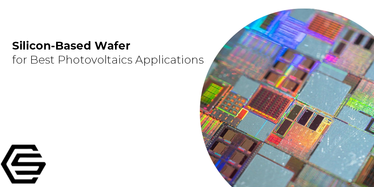
Silicon-Based Wafer for Best Photovoltaics Applications

Properties of Silicon
Silicon is mostly used for commercial purposes with slight processing and purification including silica sand, stone, and clays. It engages in reactions with over 60 elements to produce different compounds. The main component of most semiconductors, cement, ceramics, and glass is silicon. Silicon is a significant component of steel and is commonly used in bricks for the construction industry. Based on silicon’s metalloid nature, the intermetallic compounds of silicon are used in alloy industries to make them resistant to metals like copper, magnesium, and aluminum. The higher assays of 99% in metallurgic silicon have applications in silicon resins, seals, and oils. Thin silicon crystals are used in the photovoltaic cell to directly conserve energy in solar cells and piezoelectric glasses take the advantage of silicon crystals. The most common crystalline form of silicon was prepared by electrolyzing aluminum chloride and sodium chloride along with 10% silicon. Since this method was a bit expensive, a more cost-effective was developed later. The chemical research on crystal silicon production kept on which led to the discovery of volatile silicon hydrides, synthesized silane, and trichlorosilane. It was in the 20th century that the structure and composition of silicate were elucidated.
Wafers which are also referred to as a slice of a substrate, are thin layers of a semiconductor applied mostly in integrated circuits fabrication, photovoltaic cells, and solar cell manufacturing. Wafers have a significant role as substrates for devices in microelectronic scales. In order to be applied, wafers undergo modifications including ion implantation, doping, thin film deposition, and etching.
To learn more about silicon wafers and their applications,
you can read our blog post here.
Photovoltaics
Photovoltaics are considered a prime source of sustainable energy in addition to other renewable energy sources. Primarily, photovoltaic cells are based on silicon in today's technology. Particularly, silicone is employed in photovoltaic cells in order to produce monocrystalline and multi-crystalline wafers as well as to develop thin film silicon modules for a series of favorable applications. Solar cell manufacturing is highly dependent on crystalline silicon wafers therefore, the technology based on silicon wafers is regarded as a highly crucial issue for photovoltaics today. The price per Watt Peak (Wp) through the direct conversion of sunlight to electricity using solar cells based on wafers decrease is regarded as vital as the efficiency of conversion increases as a result of a deeper understanding and recognition of the factors involved in the conversion process. These outcomes are achieved by taking the advantage of process research and proper materials as well as dedicated development of technologies to get over the expenses in the past few years. Basically, photovoltaics deals with the ways and approaches to lower the fabrication costs per Watt peak. The cost shares of multi-crystalline solar systems per Watt peak are estimated as solar cell processing 13%, PV-system and convertor cost 30%, solar module processing 9%, solar grade silicon 20%, and solar ingot 28% altogether.1
Industrial Silicon Wafer Solar Cells
During the last decade, more than 80% of wafer-based silicon solar cells were manufactured according to screen printing technique to form the silver front and aluminum rear contacts taking advantage of chemical vapor deposition to grow silicon nitride as an antireflection agent to be employed on the front surface. Most of the common printed solar cells in today's industry apply the process which comprises a relatively small amount of processing steps. In fact, process equipment in this class of solar cells is available commercially together with numerous different equipment. Accordingly, the standard screen-printed solar cell has reached average efficiencies of over 15% in the case of multi-crystalline and nearly 16.5 in the case of Czochralski silicon in industrial production.